According to information from Zhong Tung Online, a research team at the University of Tokyo, Japan, has recently made a significant breakthrough in the field of nanomaterials. Using boron nitride (BN) nanotubes as a supporting template, they successfully constructed single-walled molybdenum disulfide nanotubes with a diameter of only about 1 nanometer. This size is roughly one hundred thousandth the diameter of a human hair, setting a new global record for the smallest semiconductor material and laying the foundation for exploring the properties of materials at extreme scales.
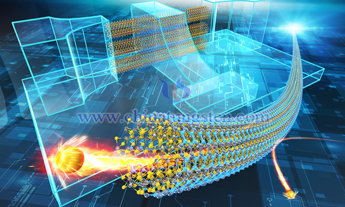
During the experiment, researchers used the confined space inside the BN nanotubes as a reaction environment to guide the orderly assembly of MoS? atoms, ultimately obtaining ultrafine single-walled MoS? nanotubes with uniform structure and clear atomic arrangement. The research team pointed out that the restricted space not only facilitates the formation of such ultra-small structures but also significantly enhances material uniformity and crystallinity.
Further analysis showed that as the nanotube diameter decreases, its electronic band structure changes noticeably, with the bandgap showing a downward trend. These experimental results closely match theoretical predictions made about 25 years ago, providing strong experimental verification for the related theory.
Currently, semiconductor devices are continuously moving toward smaller scales, but traditional manufacturing processes often produce structural defects during miniaturization, affecting device performance. In contrast, MoS? nanotubes demonstrate unique advantages in size control and atomic structural uniformity, making them promising candidates for channel materials in future ultra-miniature electronic devices.
However, industrial application of this technology still requires further breakthroughs. The currently prepared nanotubes only reach lengths of several hundred nanometers. In the next stage, the research team plans to extend the length to about 1 micrometer and attempt to apply this preparation strategy to other inorganic nanomaterial systems, including nanotubes with magnetic or superconducting properties, opening up more possibilities for developing new functional devices.


